Research plan for
HiPerFPGA
Introduction
The shrinking line width of semiconductor manufacturing processes has increased the challenges of digital system designers, since the design complexity increases quadratically compared to a linear decrease in the line width. This has motivated research into modular design methods, rapid prototyping and distributed systems.
Most design efforts in communications technology, consumer electronics and medical electronics are dedicated to software development. A side effect of this phenomenom is that the underlying hardware platform may not be optimal for a particular application, since it was originally designed for a different application. Rapidly changing standards and the demand for new applications cannot tolerate the limitations of the conventional fixed and rigid Microprocessor/ASIC design approach.
There is clearly a need for universal platforms, and future electronics must incorporate reprogrammability at the device level. Field Programmable Gate Arrays (FPGAs) are ideal components in this respect, as they can be reprogrammed within a fraction of a second.
Dynamic and partial reprogramming of system components can also increase the performance of electronics systems. This requires advanced design methods, since support for partial reprogrammability has not yet found adequate support in design tools. Furthermore, software-based design methods need to be emphasized also in electronics research.
The Internet has changed the world in many ways during the last decade, but its capabilities as a transport medium in distributed computing have remained mostly untapped. Especially small- to medium-sized Ethernet-based TCP/IP networks are attractive alternatives for connecting together reprogrammable computation acceleration units.
Based on the preceding observations, an Internet-connected distributed FPGA-based cluster (HiPerFPGA) is being proposed as a solution for computationally intensive applications.
HiPerFPGA—the Hardware
Platform
FGPAs have traditionally been used as coprocessors to alleviate the load of the host processor by performing dedicated and highly specialized computation tasks. This is called processor off-loading and the term hardware accelerator has been used for the FPGA-based coprocessor.
As additional computation acceleration is required, the limiting factor becomes the amount of available logic elements[1] (LEs) in the FPGA. A traditional solution to overcome limitations in FPGA size has been to use multiple FPGAs in the hardware accelerator. This approach is inflexible, since only the amount of required LEs for a particular application with fixed specifications is available. When another application is designed for the hardware accelerator, the available LEs may no be sufficient, and a design cycle has to be initiated.
When a generic computation platform is required, it is not possible to estimate the needed resources beforehand. Using the same idea as in networked computer clusters, it turns out that a flexibly expandable networked FPGA cluster with dynamic resource allocation solves the problems inherent in fixed-sized FPGA-based calculation systems.
The proposed FPGA cluster is called HiPerFPGA (High-Performance FPGA) and contains several FPGA-based computation units, called FPGA Nodes, each with a 100Mbps Ethernet network adapter. The FPGA Nodes are fully connected to each other through an Ethernet switch. Since Ethernet is a core technology in modern Internet, it is also a cost-effective solution for high-speed communication. Integration to other systems is also straightforward. Furthermore, the upper limit of fully FPGA Nodes units is for all practical purposes infinite.
The FPGA Nodes provide all the computation power of the HiPerFPGA. The Master Node computer handles resource allocation and load balancing. The Master Node also supplies the computation data for all FPGA Nodes and collects the results when the computation cycle is finished. To avoid bottlenecks in multiple accesses from the Master Node to the FPGA Nodes, a 1 Gbps Ethernet interface is to be used. Since communication between the Master Node and the FPGA Nodes is synchronized, the 1 Gbps connection can be fully utilized with 10 simultaneous 100 Mbps connecetions.
Distributed FPGA designs are not currently supported by commercial design tools, and custom-made design tools and plugins for development platforms are needed. A lot of work needs to be done to overcome this limitation, but the goal is to hide the underlying achitecture and make the design flow similar to a single chip design. The HiPerFPGA can be viewed as a single scalable very high capacity FPGA from the designer’s point of view. This is a key factor in making the design flow for massively parallel systems a reasonable task.
The HiPerFPGA is partially reprogrammable by reprogramming a single or more FPGA Nodes. In other words, the HiPerFPGA has the ability to change a portion of the design whilst the remainder of the cluster continues to operate. This is an extension of the more traditional SoC (System on a chip) technology, where spatial resource binding takes place at design time.
An FPGA Node includes one or two FPGAs, an Ethernet interface, and memory. A generic card should have the fastest and the largest chips available. This way, algorithm development is not limited by hardware. Although memory in an FPGA Node is not necessary in every application, a generic card needs memory.
Since the goal is to have computing power through size and as a Printed Circuit Board (PCB) cannot be too big for manufacturing reasons, there is additional motivation for clustering. When the HiPerFPGA is connected to the Internet, it would be on everyone’s use for short but extensive computations. A potential business application would be to sell the computational resources of the HiPerFPGA over the Internet.
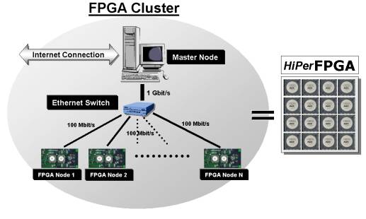
Figure 1 A general block diagram of the HiPerFPGA with its inner structure and network connections
Applications of the
hardware platform
As the HiPerFPGA is a universal hardware platform, practically every conceivable application can or could be implemented on it. Computing models based on parallelism and partial reprogramming of the HiPerFPGA should yield massive speedups when compared to a traditional sequential microprocessor-based implementation. The research project will concentrate on the following application areas to validate the feasibility and relevance of using a massively parallel and distributed reprogrammable platform as an accelerator: digital signal processing (DSP) algorithms, string matching in bioinformatics, statistical problems in computational physics, cryptanalysis, nonlinear optimization methods in evolutionary computation and neural network -based peer-to-peer (P2P) resource discovery algorithm verification. A brief overview of the application areas is presented in the following paragraphs. The challenge is to describe the computation tasks in a hardware description language (VHDL, for example) and to perform partial reprogramming of the HiPerFPGA to maximize its performance.
Three goals
have driven the development of DSP implementations: data parallelism,
application-specific specialization and functional flexibility. A
reprogrammable platform suits all these requirements, as an abundance of
programmable logic facilitates the creation of numerous functional units
directly in hardware. Reprogrammable platforms can be quickly updated based on
application demands without manual upgrades or hardware swaps. Standard DSP
algorithms, such as the Discrete Fourier Transform (DFT) and mathematical
algorithms, such as inverting huge matrices, will be tested on the HiPerFPGA
and the implementation efficiency in terms of speedup and cost will be
evaluated.
An
interesting interdisciplinary application of future electronics lies in the
emerging field of bioinformatics, where the ability to rapidly search large
databases of genetic information is becoming increasingly important. With the
expected completion of the Human Genome Project in 2003, the amount of data to
be searched, as well as the number of searches being performed on this data
will increase dramatically. The basic challenge in this application is string
matching, where two arrays of characters are compared to determine their
similarity. A highly parallel and distributed computing environment consisting
of n discrete nodes can divide the string matching task to n
discrete simultaneous tasks. It is possible, that the HiPerFPGA can achieve
speedups of several orders of magnitude.
Although
analytical methods exist to tackle many-body statistical problems, they are limited
in scope and do not work well when applied to even medium-sized systems. Monte
Carlo tehcniques are typically used in such cases to simulate truncated
versions of these systems. This has traditionally required enormous computing
resources. If the system under simulation (typically a grid or a mesh) is
mapped directly to the HiPerFPGA, its simulation time may decrease drastically.
Random number generators are needed in stochastic simulations, and these can be
implemented in an area-efficient manner on the FPGA Nodes.
Linear cryptanalysis is a technology that takes advantage of
possible input-output correlations of a cipher. Evaluating this relationship
for a sufficient number of plaintext/ciphertext pairs, it is possible to
recover some bits of the key faster than an exhaustive search. The research
project will experiment with and expand on the implementations of linear
cryptanalysis methods used in a hardware-assisted DES (Digital Encryption
Standard) with a goal of minimizing the key retrieval time.
Evolutionary computation mimics the processes of biological evolution with its ideas of natural selection and survival of the fittest to provide effective solutions for optimization problems. Genetic algorithms (GAs) are probably the best-known approach to evolutionary computation. Massively parallel GA implementations may yield speedup factors of several orders of magnitude compared to software-based approaches, as the unusual word lengths, bit-level atomary operations and inherent parallelism of GAs can take full advantage of the underlying reprogrammable platform.
Peer-to-peer (P2P) computing and networking requires mechanisms that are aware of and utilize a global space of computational resources to provide facilities for efficient lookup, wide-area programming, security and fault tolerance. The mathematically oriented research at Jyväskylä University on P2P resource discovery with neural networks can be implemented and verified on the HiPerFPGA, since the speedup factor between hardware and software-based neural network implementations may be several orders of magnitude.
Research Consortium
(HUT-JyU)
Professor Jorma
Skyttä (Signal Processing Laboratory, Helsinki University of Technology) will manage
the research consortium. Lic. Tech.
Matti Tommiska, whose
doctoral dissertation is expected to take place in summer 2003, will assist
professor Skyttä as a postdoc researcher and project manager.
The following four Ph.D. students will complete their doctoral dissertation under professor Skyttä’s supervision during the three-year research period: Juha Forsten, Esa Korpela, Antti Hämäläinen and Kimmo Järvinen. All researchers have attained solid previous experience on their respective fields of study in their M.Sc. projects.
Professor Jarkko Vuori (Department of Mathematical
Information Technology, University of
Jyväskylä) will supervise Ph.D. student Mikko Vapa, with the goal of
finishing doctoral studies on P2P resource discovery in 2006.
The primary
added value of the research consortium is that the HiPerFPGA platform provides
an excellent testbed for neural networks -based P2P resource discovery
algorithms. The research consortium will co-operate closely with electronic
means (E-mail, WWW and regular meetings.
The project
may also employ M.Sc. students, especially in Master Node control software
development and hardware-related design tasks.
The
HiPerFPGA may also have applications in the Tekes-funded Brocom project
(accelerating radio resource management algorithm simulation) and GO++ project
(linear cryptanalysis of A5/1 encryption).
Timetable
The preliminary timetable of the research
project is presented below.
|
2003 |
Construction of the hardware platform begins
with the goal of achieving Ethernet connectivity, applications are studied
and coded in VHDL |
|
2004 |
First version of the hardware platform is
ready, applications implemented on the platform, first results of speedup
achieved |
|
2005 |
Second version of the hardware platform with full
Internet connectivity is ready, potentially globally distributed applications
are tested |
|
2006 |
Additional improvement of the platform, five
Ph.D. thesis are finished. |
Objectives
The primary
goal of the research project is to attain knowledge of the characteristics and
applicability of reprogrammability in future electronics. This is coupled with
basic research into distributed and parallel methods for accelerating
computation in a cost-effective manner.
The
academic goal is five Ph.D. dissertations (4 at HUT, 1 at JyU) during the
three-year research period. In addition, approximately one M.Sc. thesis per
year will be written.
Scientific
patents will be applied to protect the immaterial rights of the inventor(s), if
the research project produces innovative and patentable results.
The
research project will disseminate its results by publishing articles in
international scientific journals and conferences. The research project will
also continuously maintain its own web server, whose address is http://hiperfpga.hut.fi/.